- 您现在的位置:买卖IC网 > Sheet目录3515 > LTC2050HVHS6#TRM (Linear Technology)IC OP AMP ZERO-DRIFT SOT23-6
LTC2050/LTC2050HV
4
2050fc
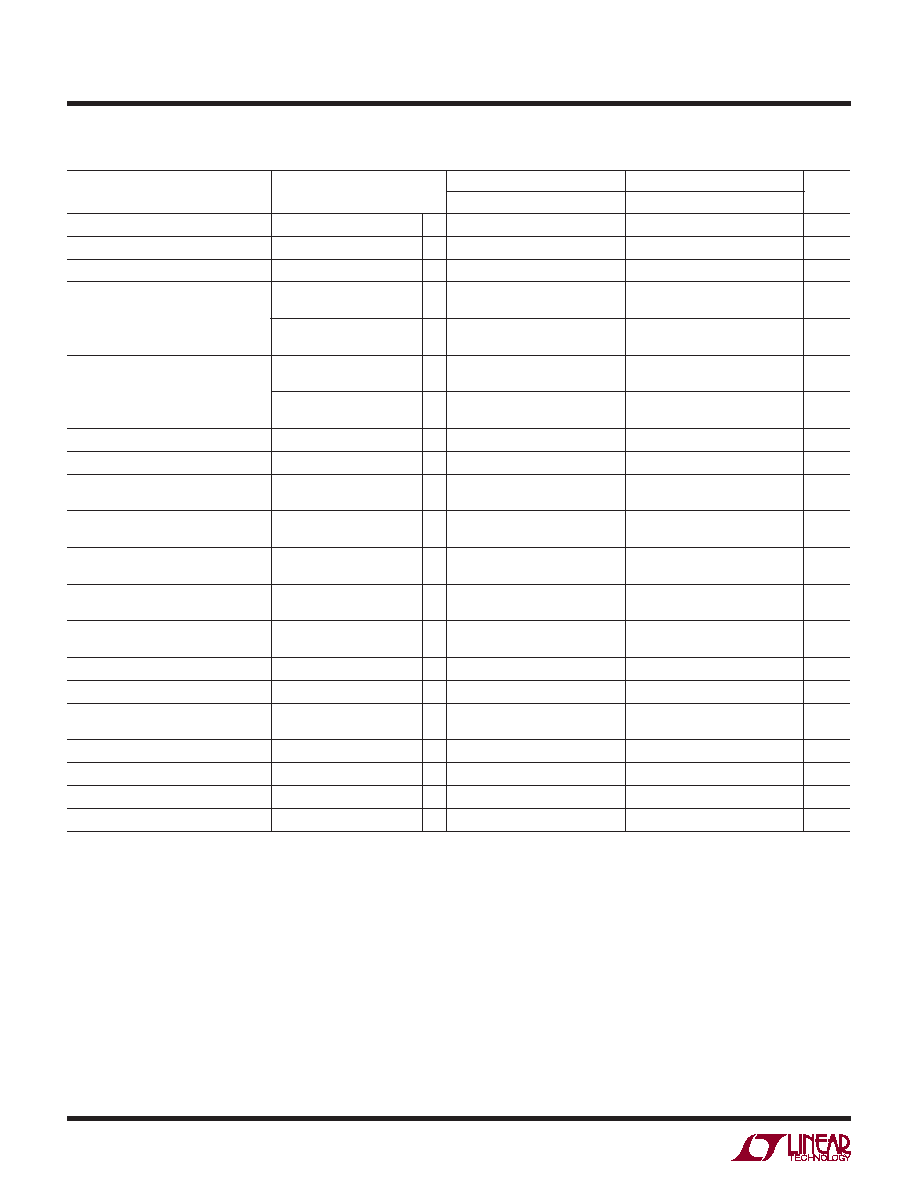
ELECTRICAL CHARACTERISTICS
PARAMETER
CONDITIONS
C, I SUFFIXES
H SUFFIX
UNITS
MIN
TYP
MAX
MIN
TYP
MAX
Input Offset Voltage
(Note 2)
±0.5
±3
±0.5
±3
μV
Average Input Offset Drift
(Note 2)
l
±0.03
±0.05
μV/°C
Long-Term Offset Drift
50
nV/√mo
Input Bias Current
LTC2050
l
±20
±75
±300
±20
±75
±4000
pA
LTC2050HV
l
±1
±50
±100
±1
±50
±4000
pA
Input Offset Current
LTC2050
l
±150
±200
±150
±1000
pA
LTC2050HV
l
±100
±150
±100
±1000
pA
Input Noise Voltage
RS = 100Ω, 0.01Hz to 10Hz
1.5
μVP-P
Input Capacitance
1.7
pF
Common Mode Rejection Ratio
VCM = GND to (V+ – 1.3)
l
115
110
130
115
110
130
dB
Power Supply Rejection Ratio
VS = 2.7V to 6V
l
120
115
130
120
115
130
dB
Large-Signal Voltage Gain
RL = 10k
l
120
115
140
120
115
140
dB
Output Voltage Swing High
RL = 2k to GND
RL = 10k to GND
l
2.85
2.95
2.94
2.98
2.85
2.95
2.94
2.98
V
Output Voltage Swing Low
RL = 2k to GND
RL = 10k to GND
l
1
10
1
10
mV
Slew Rate
22
V/μs
Gain Bandwidth Product
3
MHz
Supply Current
VSHDN = VIH, No Load
VSHDN = VIL
l
0.75
1.1
10
0.75
1.2
10
mA
μA
Shutdown Pin Input Low Voltage (VIL)
l
V– + 0.5
V
Shutdown Pin Input High Voltage (VIH)
l
V+ – 0.5
V
Shutdown Pin Input Current
VSHDN = GND
l
–0.5
–3
–0.5
–3
μA
Internal Sampling Frequency
7.5
kHz
(LTC2050/LTC2050HV) The
l denotes the specications which apply over
the full operating temperature range, otherwise specications are at TA = 25°C. VS = 3V unless otherwise noted. (Note 3)
发布紧急采购,3分钟左右您将得到回复。
相关PDF资料
LTC6079CDHC#TRPBF
IC OP AMP QUAD R-R I/O 16DFN
MAX9922EUB+
IC AMP CURRENT SENSE 10-MSOP
LTC6079CDHC#TR
IC OP AMP QUAD R-R I/O 16DFN
MAX4252ESA+
IC OPAMP R-R LN DUAL 8-SOIC
RMCF0805FT13K7
RES 13.7K OHM 1/8W 1% 0805 SMD
MMS-128-02-L-DH
CONN RCPT 2MM 56POS DL HORZ SMD
929838-02-25
CONN HEADER .100 DUAL R/A 50POS
TSW-133-08-S-S-RA
CONN HEADER 33PS .100 SGL R/A AU
相关代理商/技术参数
LTC2050HVHS6#TRMPBF
功能描述:IC OP AMP ZERO-DRIFT SOT23-6 RoHS:是 类别:集成电路 (IC) >> Linear - Amplifiers - Instrumentation 系列:- 标准包装:100 系列:- 放大器类型:通用 电路数:1 输出类型:- 转换速率:0.2 V/µs 增益带宽积:- -3db带宽:- 电流 - 输入偏压:100pA 电压 - 输入偏移:30µV 电流 - 电源:380µA 电流 - 输出 / 通道:- 电压 - 电源,单路/双路(±):±2 V ~ 18 V 工作温度:0°C ~ 70°C 安装类型:表面贴装 封装/外壳:8-SOIC(0.154",3.90mm 宽) 供应商设备封装:8-SO 包装:管件
LTC2050HVHS6#TRPBF
功能描述:IC OPAMP ZERO-DRIFT SOT23-6 RoHS:是 类别:集成电路 (IC) >> Linear - Amplifiers - Instrumentation 系列:- 标准包装:50 系列:- 放大器类型:通用 电路数:2 输出类型:满摆幅 转换速率:1.8 V/µs 增益带宽积:6.5MHz -3db带宽:4.5MHz 电流 - 输入偏压:5nA 电压 - 输入偏移:100µV 电流 - 电源:65µA 电流 - 输出 / 通道:35mA 电压 - 电源,单路/双路(±):1.8 V ~ 5.25 V,±0.9 V ~ 2.625 V 工作温度:-40°C ~ 85°C 安装类型:表面贴装 封装/外壳:10-TFSOP,10-MSOP(0.118",3.00mm 宽) 供应商设备封装:10-MSOP 包装:管件
LTC2050HVHS6-PBF
制造商:LINER 制造商全称:Linear Technology 功能描述:Zero-Drift Operational Amplifi ers in SOT-23
LTC2050HVHS6-TR
制造商:LINER 制造商全称:Linear Technology 功能描述:Zero-Drift Operational Amplifi ers in SOT-23
LTC2050HVHS6-TRPBF
制造商:LINER 制造商全称:Linear Technology 功能描述:Zero-Drift Operational Amplifi ers in SOT-23
LTC2050HVIS5
制造商:Linear Technology 功能描述:SP Amp Zero Drift Amplifier Single R-R O/P 制造商:Linear Technology 功能描述:SP Amp Zero Drift Amplifier Single R-R O/P ±5.5V/11V 5-Pin TSOT-23 制造商:Linear Technology 功能描述:Zero Drift Op Amp
LTC2050HVIS5#PBF
制造商:Linear Technology 功能描述:SP Amp Zero Drift Amplifier Single R-R O/P 制造商:Linear Technology 功能描述:OP AMP 11V 3MHZ 2V/US 5TSO
LTC2050HVIS5#TR
功能描述:IC OPAMP ZERO DRIFT HV TSOT23-5 RoHS:否 类别:集成电路 (IC) >> Linear - Amplifiers - Instrumentation 系列:- 标准包装:1,000 系列:- 放大器类型:电压反馈 电路数:4 输出类型:满摆幅 转换速率:33 V/µs 增益带宽积:20MHz -3db带宽:30MHz 电流 - 输入偏压:2nA 电压 - 输入偏移:3000µV 电流 - 电源:2.5mA 电流 - 输出 / 通道:30mA 电压 - 电源,单路/双路(±):4.5 V ~ 16.5 V,±2.25 V ~ 8.25 V 工作温度:-40°C ~ 85°C 安装类型:表面贴装 封装/外壳:14-SOIC(0.154",3.90mm 宽) 供应商设备封装:14-SOIC 包装:带卷 (TR)